
Object. To study the characteristics of NPN transistors in Common Emitter configuration.
Apparatus. NPN transistor, voltmeters, milliammeter, microammeter, variable DC supply, resistors of suitable values and connection leads.
Theory. The transistor is a three-terminal solid – state device which regulates current or voltage flow and acts as a switch or gate for signals and is formed by connecting two diodes back-to-back. Hence it has got two PN junctions. Three terminals are drawn out of the three semiconductor materials present in it. This type of connection offers two types of transistors, namely, PNP and NPN which means an N-type material between two P types and the other is a P-type material between two N-types respectively. The three terminals drawn from the transistor are Emitter, Base and Collector terminals which function as discussed below.
The Emitter has a moderate size and is heavily doped as its main function is to supply large number of majority carriers, i.e., either electrons or holes. As this emits electrons, it is called as an Emitter. This is simply indicated with the letter E. The Base is the middle portion of a transistor which is thin and lightly doped. Its main function is to pass the majority carriers from the emitter to the collector. This is indicated by the letter B. The Collector is a bit larger in size than emitter and base. Its function is to collect all the majority charge carriers flowing from the emitter through the base towards it. It is moderately doped. This is indicated by the letter C.
The operation of an NPN transistor can be explained by fig. 2, in which emitter-base junction is forward biased and collector-base junction is reverse biased which is the active state of the transistor.
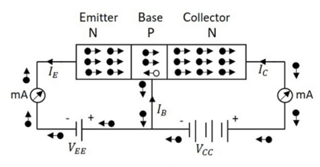
The voltage VEE provides a negative potential at the emitter which repels the electrons in the N-type material and these electrons cross the emitter-base junction constituting the emitter current IE, to reach the base region. There is a very low concentration of electrons that recombine with free holes of P-region. This provides very low current which constitutes the base current IB. The remaining holes cross the collector-base junction, to constitute the collector current IC. As an electron reaches out of the collector terminal, and enters the positive terminal of the battery, an electron from the negative terminal of the battery VEE enters the emitter region. This flow slowly increases and the electron current flows through the transistor.
In common emitter configuration, the emitter is common to both input and output terminals of the circuit. The input characteristics are a plot between base current IB and base – emitter voltage VBE keeping collector voltage VCE constant as shown in fig. 2. Since the base-emitter section of a transistor is a diode, this curve resembles that of a simple p-n junction diode curve in forward bias.
Procedure. (Not to be written in copy)
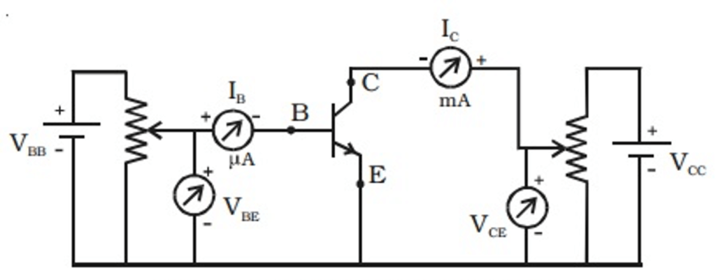
The experimental circuit to plot the characteristics of an NPN transistor in CE configuration is given in fig. 1.
Connect the following only in NPN circuit.
1. Base circuit: Connect terminals 1-1, 2-2, 3-3, 4-4, 11-11 & 12-12 (if any).
2. Collector circuit: Connect terminals 5-5, 6-6, 7-7, 8-8, 9-9 & 10-10.
3. Switch on the power supply.
Input characteristics
4. Keep collector – emitter voltage (VCE) constant at 0 volt and increase base- emitter voltage VBE in steps of 0.1 V to 0.5 V and record VBE & IB for each step. Now increase VBE in steps of 0.02 V (division by division) and record VBE & IB for each step upto IB = 400 μA.
5. Repeat step 4 for other higher constant values of VCE say 2V and 4V. Record observations in the table given below.
Least count of Voltmeter measuring VBE = ………………….
Least count of Voltmeter measuring VCE = ………………….
Least count of Ammeter measuring IC = ……………………
Least count of Ammeter measuring IB = …………………..
6. Plot a graph between VBE on X- axis and IB on Y-axis for constant values of VCE= 0 V and 4 V as shown in fig. 3.
7. As shown in fig. 3, calculate input dynamic resistance ri using the following equation:
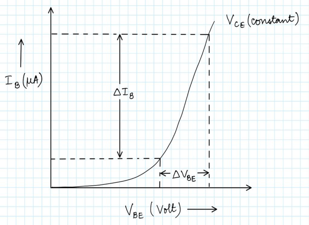
\[
r_i = \frac{\Delta V_{BE}}{\Delta I_B} \text{ at constant } V_{CE}.
\]
Output characteristics
8. Keep base current IB constant say, 100 μA and increase collector – emitter voltage VCE in steps of 0.1 V upto 0.5 V and record VCE and collector current IC for each step. Now increase VCE in steps of 0.5 V and record the VCE & IC for each step.
9. Repeat step 8 for other higher constant values of IC say 200 μA, 300 μA, and 400 μA. Record observations in the table given below.
Least count of Voltmeter measuring VBE = ………………….
Least count of Voltmeter measuring VCE = ………………….
Least count of Ammeter measuring IC = ………………….
Least count of Ammeter measuring IB = ………………….
| S.No. | IB = 100 (μA) | IB = 200 (μA) | IB = 300 (μA) | IB = 400 (μA) | ||||
| VCE (V) | IC (mA) | VCE (V) | IC (mA) | VCE (V) | IC (mA) | VCE (V) | IC (mA) | |
| 1. | 0 | 0 | 0 | 0 | ||||
| 2. | 0.1 | 0.1 | 0.1 | 0.1 | ||||
| 3. | 0.2 | 0.2 | 0.2 | 0.2 | ||||
| 4. | 0.3 | 0.3 | 0.3 | 0.3 | ||||
| 5. | 0.4 | 0.4 | 0.4 | 0.4 | ||||
| 6. | 0.5 | 0.5 | 0.5 | 0.5 | ||||
| 7. | 1.0 | 1.0 | 1.0 | 1.0 | ||||
| 8. | 1.5 | 1.5 | 1.5 | 1.5 | ||||
| 9. | 2.0 | 2.0 | 2.0 | 2.0 | ||||
| 10. | 2.5 | 2.5 | 2.5 | 2.5 | ||||
| 11. | 3.0 | 3.0 | 3.0 | 3.0 | ||||
| 12. | 3.5 | 3.5 | 3.5 | 3.5 | ||||
| 13. | 4.0 | 4.0 | 4.0 | 4.0 | ||||
| 14. | 4.5 | 4.5 | 4.5 | 4.5 | ||||
10. Plot a graph between VCE on X- axis and IC on Y-axis for constant values of IB= 100 μA, 200 μA, 300 μA, and 400 μA as shown in fig. 4.
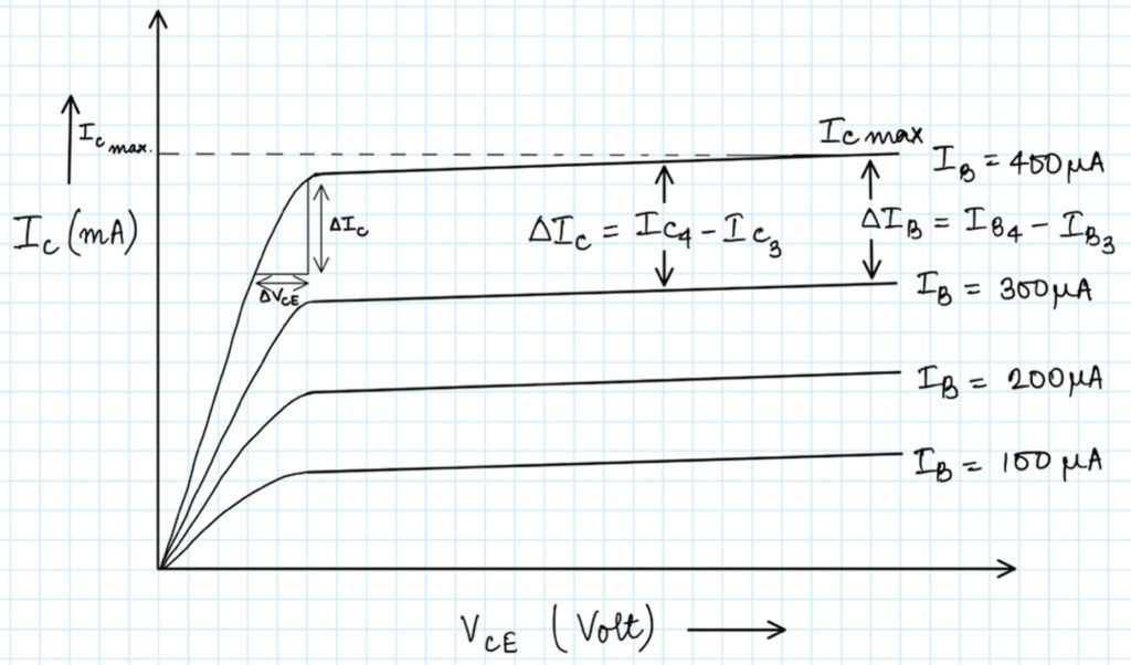
11. As shown in fig. 4, calculate output dynamic resistance ro, βdc and βac following relations:
\[
r_o = \frac{\Delta V_{CE}}{\Delta I_C} \text{ at constant } I_B \\
\text{DC current gain } \beta_{dc} = \frac{I_{C(\text{max})}}{I_B} \\
\text{AC current gain } \beta_{ac} = \frac{\Delta I_C(I_{C4}-I_{C3})}{\Delta I_B(I_{B4}-I_{B3})}
\]
Results.
- Input dynamic resistance ri = …………………
- Output dynamic resistance ri = …………………….
- DC current gain βdc = ……………………
- AC current gain βac = ……………………
Precautions.
1. The emitter-base junction is kept in forward bias, while the collector-emitter junction is kept in reverse bias.
2. A high potential should not be applied at the base or collector.
3. The transistor should not be kept on for a long duration. For this, a separate key should be connected to the battery both in the base circuit as well as in the collector circuit.
4. The + ve marked terminals of the milliammeter or microammeter and voltmeter should always be connected to the positive terminal of the battery.
Viva – Voce
Q. What is a junction transistor?
Ans. It is a small device composed of P and N type silicon (or germanium) semiconductors which can be used like a triode valve. It is constructed by joining three layers of P and N type semiconductors. These three semiconducting layers are called respectively the emitter, base and collector. The middle semiconductor layer is kept very thin and is always the base and the remaining layers on the either side are emitter and collector.
Q. Can you distinguish the emitter, base and collector electrode (or terminal) just by seeing the transistor?
Ans. There is either a red dot marked at the collector, or the collector terminal is more separated from the middle (base) terminal than the emitter terminal.
Q. Why is a junction transistor also called BJT?
Ans. BJT means bipolar junction transistor. The reason is that both the electrons and holes take part in the operation of a transistor.
Q. What is a semiconductor? Give two examples.
Ans. The tetravalent elements are called the semi-conductors. At ordinary temperatures they are insulators but on heating them, the electric conduction becomes possible through them at a high temperature (i.e., their resistance decreases, or the conductivity increases on increasing the temperature). Silicon and germanium are examples of semiconductors.
Q. What do you mean by P and N type semiconductors?
Ans. P and N type semiconductors are the extrinsic semi- conductors. When impurity of trivalent atoms (such as Al, In) is mixed with pure semiconductor, we get P type semiconductor. The impurity ions are called the acceptor ions. On the other hand, if the impurity of pentavalent atoms (such as As, Sb) is mixed with pure semiconductor, we get N type semiconductor. The impurity ions are called the donor ions.
Q. What are responsible for the flow of current in an N type semi – conductor: electrons or holes?
Ans. Electrons.
Q. What are the majority current carriers in the P and N type semi-conductors?
Ans. In P type semiconductor the majority current carriers are the holes, while in N type semiconductor the majority current carriers are the electrons.
Q. Why is a transistor so named?
Ans. The word transistor means transfer of resistance. Since the emitter-base junction is in forward bias and the collector-base junction is in reverse bias, therefore the resistance of emitter-base junction is very low while that of collector-base junction is very high. In other words, the resistance of emitter-base junction is transferred to the collector-base junction.
Q. How many types of transistors are there?
Ans. There are two types of transistors. They are: (i) NPN type and (ii) PNP type.
(i) NPN type: There are the layers of N type semiconductors on either side of a thin P type semiconductor layer. In it, emitter is N type, base is P type and collector is N type.
(ii) PNP type: There are the layers of P type semiconductors on either side of a thin layer of N type semiconductor. In I,t emitter is P type, base is N type and collector is P type.
Q. Why is the base of transistor kept thin and is doped with less impurity?
Ans. So that only a small number of charge carriers coming on base from the emitter may combine with the majority charge carriers present in the base.
Q. Can a transistor be used with 220 V D.C.?
Ans. No. When the reverse voltage at the collector-emitter junction exceeds the Zener voltage, the transistor becomes useless.
Q. How can you detect whether a transistor is still functional or it has become useless?
Ans. Keeping each junction of the transistor once in forward bias and then in reverse bias, its resistance is measured. If the resistance in reverse bias is much large than in the forward bias, the transistor is functional, otherwise it has become useless.
Q. Is it possible to obtain an NPN transistor by keeping the two N-P junction diodes in N-P and P-N order?
Ans. No, because then the base (P type) will become very thick.
Q. Is it possible to keep the emitter in the reverse bias and the collector in the forward bias?
Ans. No. The reason is that in this condition, the majority charge carriers from emitter will not be able to go to the base or collector.
Q. Is it possible to keep the emitter and collector both in the forward bias?
Ans. No. In this condition, the charge carriers of emitter will move from emitter to the base, but the charge carriers of collector instead of going from base to the collector will move from collector to the base. In this case, the transistor will work in saturation state.
Q. Is it possible to keep both the emitter and collector in reverse bias?
Ans. No, because in this condition, the charge carriers will not be able to reach from emitter to base. In this case, the transistor will work in cut-off state.
Q. In which mode-CB mode or CE mode, is it advantageous to use a transistor?
Ans. In CE mode, because the current gain in CE mode is much more than in CB mode.
Q. A transistor is more useful than a triode, why?
Ans. There is no need to heat separately the electron emitter in a transistor, hence they occupy less space. There is no need to keep vacuum in them, so they are cheaper and durable. On the other hand, in a triode, electron emitter is separately heated. They occupy more space. There is vacuum in it. They are costly and their life is short.