
The voltage gain of a single stage transistor amplifier is not sufficient for many practical applications. Higher gains can be obtained by connecting a large number of amplifier stages in succession (one after the other). Resistance-capacitance (RC) coupling is most widely used to connect the output of first stage to the input (base), of the second stage and so on. It is the most popular type of coupling because it is cheap and provides a reasonably constant amplification over a wide range of frequencies.
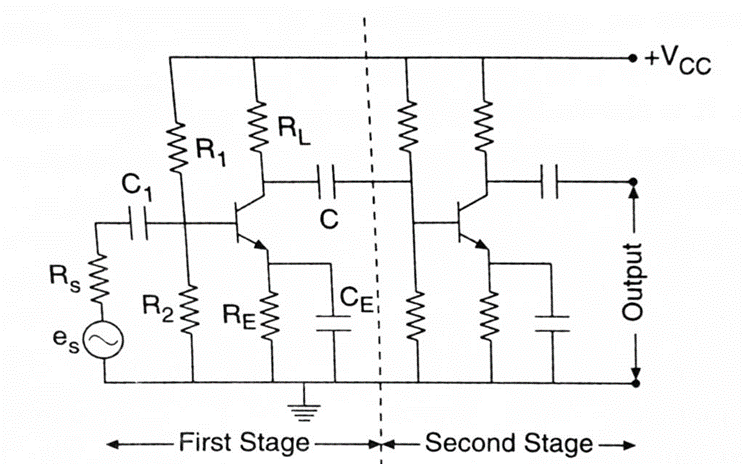
Fig. 1 shows the circuit arrangement of a two stage RC coupled CE mode transistor amplifier where resistance RL, is used as a load impedance and the capacitor C is used as a coupling element between the two stages of the amplifier.
Function of Circuit Components:
- Biasing and stabilisation network: The resistances R1, R2, and RE form the biasing and stabilisation network. It establishes a proper operating point, otherwise a part of the negative half cycle of the signal may be cut-off in the output. RE also reduces the variation of collector current with temperature.
- Input capacitor C1: Electrolytic capacitor C1 (~ 10 μF) isolates the input circuit for d.c. potentials and couples the a.c. signal voltage to the base of the transistor. If it is not used, the resistance of the signal source will be in parallel to RL and the bias voltage of the base will change.
- Emitter bypass capacitor CE: The capacitor CE connected across the emitter resistor RE is of large value (~ 100 μF) so that its reactance 1/ωCE is small. It, therefore, offers a low reactance path to the a.c. component of emitter current and thus bypasses resistor RE at audio frequencies. Consequently, the potential difference across RE is due to the d.c. component of the current only. If it is not used, the amplified a.c. signal flowing through RE will cause a voltage drop across it, thereby reducing the output voltage.
- Coupling capacitor C: The coupling capacitor C (~ 10 μF) transmits a.c. signals but blocks d.c. It couples the output of the first stage of amplifier to the input of the second stage. It blocks the d.c. voltage of the first stage from reaching the base of the second stage. Thus, the d.c. biasing of the next stage is not disturbed. For this reason, the capacitor C is also known as blocking capacitor.
Operation:
When a.c. signal is applied to the base of the first transistor, it is amplified and developed across the load resistor RL. This amplified voltage is applied to the base of next stage through the coupling capacitor C where it is further amplified and reappears across the load RL of the second stage. Thus, the successive stages amplify the signal, and the overall gain is raised to the desired level.
Frequency response curve:
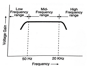
The curve representing the variation of gain of an amplifier with frequency, known as frequency response curve, is shown for a typical RC coupled amplifier in Fig. 2. It is divided into three regions. The voltage gain is substantially constant over a wide range of frequencies (middle frequency range) and decreases at low (< 50 Hz) and high (> 20 kHz) frequencies.
- At low frequencies (< 50 Hz), the gain decreases with decreasing frequency due to coupling capacitor C. As the frequency gets lower and lower, the reactance (1 /ωC) of the coupling capacitor gets higher and higher. Consequently, an increasing portion of the voltage drop takes place across C. Thus, the voltage reaching from one stage to the next stage decreases and hence the voltage gain drops. The other component due to which the gain decreases at low frequencies is the bypass capacitor C. As frequency decreases, the reactance of capacitor CE increases and becomes comparable to emitter resistance RE. Therefore, it cannot shunt the resistor RE effectively. A current passes through RE also developing an a.c. voltage. Then the effective input voltage to the amplifier i.e., the voltage between the base and emitter of the transistor, decreases. Consequently, the gain of the amplifier decreases. The lower the frequency, higher is the reactance of CE and greater is the reduction in gain.
- At mid-frequencies (50 Hz to 20 KHz), the voltage gain of the amplifier is uniform because resistor values are independent of frequency changes. As the frequency increases in this range, reactance of coupling capacitor decreases which tends to increase the gain but it simultaneously increases the loading of first stage which decreases the gain. These two factors cancel each other and hence gain at mid-frequency region remains approximately constant.
- At high frequencies (> 20 kHz), the voltage gain falls due to the capacitance that appears in shunt across the output. These capacitances consist of the collector capacitance of the transistor and the stray wiring capacitance. With increase in frequency, the reactance of these capacitors decreases and an increased part of the output is bypassed to earth. Consequently, the output voltage of the amplifier decreases and hence the voltage gain falls at high frequencies as is indicated by the bend in the curve of Fig 2. Moreover, at high frequencies, capacitive reactance of base-emitter junction is reduced. As a result, the base current increases and hence the current amplification factor β decreases.